
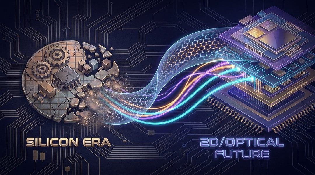
A faster processor accomplishes little when data cannot reach it efficiently. Next-generation chip design therefore involves two distinct challenges: improving electronic switches and strengthening communication between computing components.
Two-dimensional materials could help engineers build smaller transistor channels. Optical interconnects could move information between processors through light rather than electrical signals alone.
The “post-silicon era” describes this expanding engineering toolkit, not silicon’s imminent disappearance. Silicon can remain central while new materials and communication technologies address specific limitations.
Why next-generation chips need more than smaller transistors
Transistors regulate electrical current through a channel, much like controlled valves. Their gates switch that current on or off to support digital operations.
As engineers shrink devices, they must preserve reliable switching while limiting unwanted current. Improving transistor density also cannot resolve every communication bottleneck between processors.
Consider a factory with exceptionally fast machines and inadequate delivery routes. Increasing each machine’s output will not automatically improve the factory’s overall productivity.
Computing systems face a similar coordination problem. Intel identifies bandwidth, energy consumption, and communication distance as growing constraints for interconnected AI processors.
Consequently, chip designers must improve both computation and the connections supporting it.
How 2D materials could improve transistor channels
What makes an atomically thin channel useful?
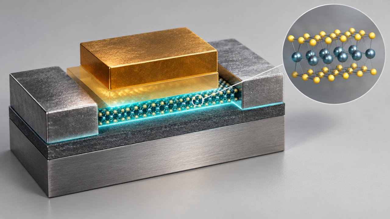
“Two-dimensional” describes an extremely thin material structure, not a processor’s overall shape. Researchers investigate these materials as alternatives for the semiconductor channels inside transistors.
Prominent candidates include molybdenum disulfide, or MoS2, and tungsten diselenide, or WSe2. Imec’s research uses these materials in complementary transistor types needed for CMOS-style integration.
Their ultrathin channels could support smaller, higher-performance transistors. However, engineers must preserve useful electrical characteristics throughout fabrication rather than assuming thinness guarantees superior devices.
What has research actually demonstrated?
In June 2026, imec, ASML, and TSMC announced complementary 2D-material transistors integrated on the same 300 mm wafer. Their devices achieved a 50 nm contacted poly pitch, a spacing measurement rather than channel thickness.
The collaboration reported 94% operational transistors under its stated electrical criterion. That result supports progress toward scalable fabrication but does not establish commercial processor yield.
This distinction matters: manufacturing working devices represents a different achievement from producing complete processors economically and reliably.
How optical interconnects move data between chips
From electrical signals to optical channels
Optical interconnects convert electronic information into optical signals for transmission. Receivers then return those signals to electrical form for electronic processing.
A simplified communication path looks like this:
Electronic processor → optical transmitter → fiber → optical receiver → electronic processor
Multiple wavelengths can carry separate channels through a shared fiber. Intel’s optical I/O demonstration used eight wavelengths and combined a silicon photonics circuit with electronic circuitry.
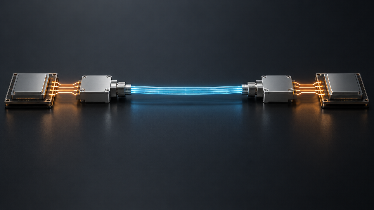
This architecture improves communication rather than replacing electronic computation with optical calculation. Silicon photonics also illustrates why “post-silicon” should not mean “silicon-free.”
Reading bandwidth and energy claims correctly
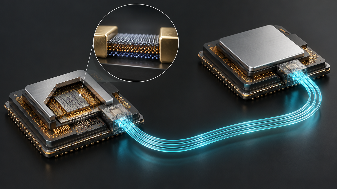
At OFC 2024, Intel demonstrated an optical I/O chiplet co-packaged with a CPU and transmitting live data. The design supports 64 channels at 32 Gbps in each direction over fiber distances up to 100 meters.
Intel reported energy consumption of 5 pJ/bit compared with approximately 15 pJ/bit for pluggable optical transceiver modules. These company-reported figures describe the communication comparison, not equivalent reductions across an entire computing system.
Practical assessments must therefore consider measurement boundaries alongside bandwidth and reach. A successful demonstration also does not establish universal commercial availability.
Where 2D materials and optical interconnects complement each other
The technologies address different architectural layers, which makes their relationship complementary rather than dependent.
In a conceptual hybrid system, candidate 2D channels would support electronic switching inside compute devices. Optical I/O would connect separate computing packages through fiber.
- Device layer: Engineers investigate alternative materials for transistor channels.
- Communication layer: Designers use optical links to transport information between computing components.
- System layer: Architects evaluate whether those improvements benefit the intended workload.
This arrangement illustrates a possible design direction, not a documented combined implementation from the demonstrations above. Neither technology requires the other to provide value.
What separates breakthroughs from everyday next-gen chips?
Readers can assess emerging chip announcements through several practical questions:
- Does the result demonstrate individual transistors or a complete operating system?
- Does fabrication support industry-scale wafers rather than isolated laboratory samples?
- Which components contribute to the reported energy measurement?
- What evidence establishes reliability, cost, and production readiness?
Imec’s research demonstrates progress in transistor integration while Intel’s example demonstrates a live optical communication link. Their achievements support different conclusions and require different manufacturing assessments.
Neither announcement alone supports a firm timetable for widespread consumer adoption.
The post-silicon era expands the chipmaking toolkit
Two-dimensional materials could improve the switches that perform electronic operations. Optical interconnects could improve the links that carry information between processors.
Their significance rests on measurable engineering outcomes rather than promises to replace silicon entirely. The strongest next-generation designs will match each technology to a specific bottleneck and demonstrate benefits across realistic systems.
For readers following semiconductor progress, that provides a useful test: examine what researchers measured before accepting what a headline predicts.