
Intel advanced packaging services gain traction with hyperscalers
Intel is in active talks with Google and Amazon to provide advanced chip packaging services for their custom AI processors. The potential agreements could mark a major step forward for Intel’s foundry push, with possible deal values reaching billions of dollars each year.
Google and Amazon already build their own AI accelerators. Google develops TPUs, while Amazon builds Trainium and Inferentia chips. Even so, they still rely on outside partners for key assembly work. That creates an opening for Intel, whose advanced packaging capabilities are now being viewed as a realistic option alongside the dominant packaging approach from Taiwan Semiconductor Manufacturing Company.
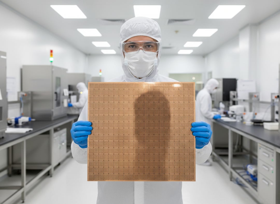
Intel’s packaging portfolio includes Embedded Multi-die Interconnect Bridge, or EMIB, and Foveros. These technologies are gaining attention at a time when supply for TSMC’s CoWoS packaging remains constrained. That supply pressure matters because advanced packaging has become a critical part of AI chip deployment, especially for large cloud providers building and scaling custom silicon.
Why Intel packaging matters for custom AI chips
Google TPU and Amazon Trainium packaging needs
Google and Amazon design powerful custom AI chips, but chip design alone is not enough. The final assembly and packaging layer is essential, especially when performance, density, and integration matter. That is where Intel is trying to position itself.
For hyperscalers, advanced packaging is not just a backend task. It is a strategic part of how AI processors are built and delivered. Intel’s EMIB and Foveros technologies give it a chance to win business from companies that need packaging capacity for increasingly complex AI hardware.
EMIB and Foveros as alternatives to CoWoS
Intel’s EMIB and Foveros offerings are emerging as credible alternatives to CoWoS. That matters because TSMC remains the dominant player in advanced packaging, but its supply is still tight. When demand is high and capacity is constrained, buyers start looking for practical second options.
Intel’s opportunity comes from being able to offer those options at a moment when custom AI chip demand is still pushing the industry hard. And for cloud companies with large-scale AI ambitions, packaging availability can become just as important as chip design itself.
A foundry lifeline for Intel
Intel’s finance chief, Dave Zinsner, pointed to the scale of the opportunity during the Morgan Stanley Technology, Media, and Telecom conference on March 5. He said the company was close to closing packaging deals worth billions of dollars per year in revenue. He also said customers were willing to prepay for capacity, a sign that Intel’s packaging services are being taken seriously.
That is a big detail. Prepayment suggests demand is not casual. It points to customers wanting to secure access before capacity fills up.
Higher margins and faster revenue from packaging
Advanced packaging also stands out because it can deliver better economics than full-wafer manufacturing agreements. Zinsner said packaging has become the more important part of Foundry today and noted that it can reach gross margins of about 40 percent.
That makes these negotiations important on two levels. First, they could bring in large revenue. Second, they could do it in a part of the business with stronger margins and quicker payoff. For Intel, that combination gives packaging an outsized role in its foundry strategy.
Geopolitical risks are strengthening Intel’s pitch
A domestic alternative to Taiwan-based capacity
Intel’s case with hyperscalers is not based only on technology. Geography is part of the pitch too. TSMC’s advanced packaging capacity is concentrated in Taiwan, and that creates supply chain and geopolitical concerns for U.S.-based cloud providers.
A domestic alternative can help reduce that risk. For companies like Google and Amazon, that kind of diversification can matter when advanced packaging has become a bottleneck tied directly to AI product rollouts.
Supply chain resilience for U.S. cloud providers
This is where Intel gains practical relevance. If large cloud providers want to reduce exposure to a single packaging hub, Intel gives them another path. The value is not only about access to advanced packaging tools. It is also about where that capacity sits and how that changes supply chain planning.
In other words, Intel is offering more than packaging capacity. It is offering an option that could help hyperscalers spread risk while supporting custom AI chip programs.
Intel capacity expansion for AI chip packaging
Intel has been building up capacity to support this opportunity. Its Project Pelican advanced packaging complex in Malaysia is expected to begin first-phase operations later this year. The site will handle die sort, preparation, and both EMIB and Foveros packaging flows.
That matters because customer interest means little without the ability to execute at scale. Project Pelican is part of Intel’s attempt to show that its packaging ambitions are backed by real operational expansion.
Malaysia Project Pelican and packaging operations
The Malaysia facility is set up to support multiple steps in the packaging process. By covering die sort, prep, and advanced packaging flows, it gives Intel a more complete operational base for serving customers that need reliable packaging throughput.
For prospective customers, capacity readiness is part of the buying decision. If Intel wants to convert negotiations into large commitments, it has to demonstrate that the infrastructure is moving into place.
EMIB production ramp with Amkor in South Korea
Intel is also expanding EMIB production through its outsourced semiconductor assembly partner Amkor at the Songdo K5 facility in South Korea. That move adds another layer to Intel’s packaging buildout and shows the company is not depending on a single site to support growth.
This broader ramp suggests Intel is preparing for meaningful packaging demand, not just talking about it.
Larger package formats could support denser AI designs
Intel has also introduced a larger 120x120mm packaging format, up from the industry-standard 100x100mm. The larger format allows for greater density of high-bandwidth memory and compute units inside a single package.
That is a notable detail because density is central to advanced AI chip design. A larger format can create more room for tightly integrated components, which is especially relevant for custom AI processors built for demanding workloads.
For companies designing accelerators at scale, packaging format is not a small engineering footnote. It can shape how much memory and compute can be brought together in one package.
When Intel could finalize packaging deals
The current timeline for finalizing customer commitments is the second half of 2026. More information is expected during Intel’s upcoming earnings call on April 23.
That leaves the discussions in an active but unfinished stage. The talks with Google and Amazon are significant already, but the real milestone will be whether Intel turns those negotiations into formal commitments.