
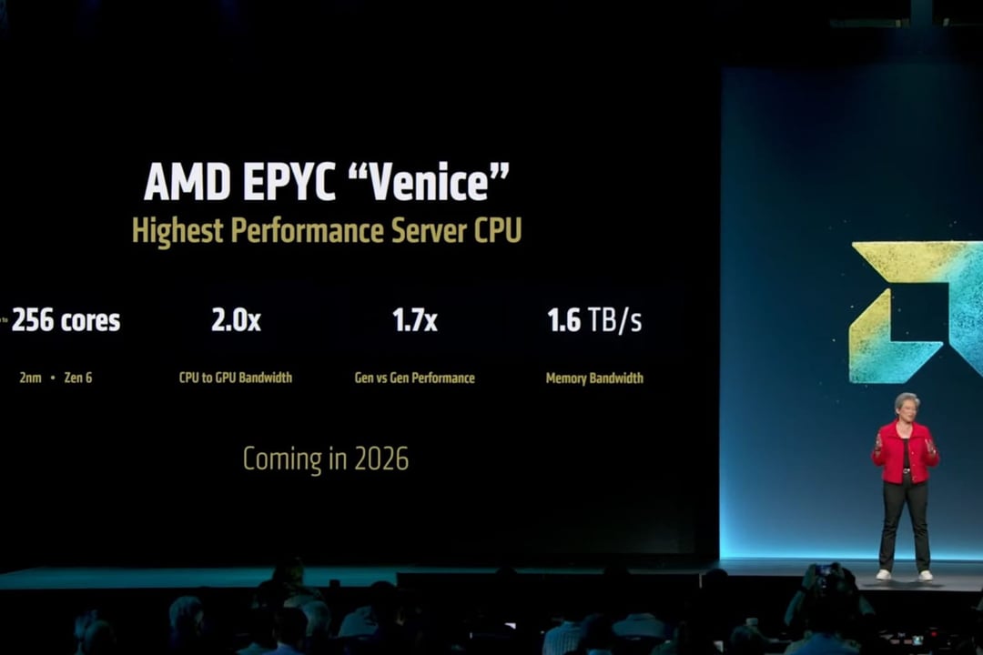
AMD used its Advancing AI 2026 keynote at San Francisco's Moscone Center to make the EPYC 9006 "Venice" family official — the company's first server processor manufactured on TSMC's 2nm process and the first commercial silicon carrying the Zen 6 architecture. CEO Lisa Su confirmed from the stage that the part is already in full production, with the first shipments scheduled to reach customers during the third quarter of 2026.
That combination matters more than either milestone would on its own. A new node buys density and efficiency; a new core architecture buys instructions-per-clock and platform features. Venice lands both in the same generation, which is why the headline core count jumped as sharply as it did.
Inside the Flagship EPYC 9996
The top-of-stack EPYC 9996 pushes to 256 Zen 6c cores and 512 threads on the fresh SP7 socket. Measured against the 192-core Turin generation it replaces, that represents a 33 percent lift in raw core count from a single package.
The layout behind that number is worth unpacking. AMD assembles the chip from eight compute chiplets, each carrying 32 dense Zen 6c cores paired with 128 MB of L3 cache. Add those together and the flagship configuration carries 1,024 MB of L3 on the package — close to triple what the previous generation offered. For workloads that live and die by cache residency, that shift is arguably more consequential than the extra cores themselves.
Memory Bandwidth and I/O
Feeding 256 cores requires a memory subsystem built to match, and AMD widened the interface accordingly. Venice runs a 16-channel DDR5 setup with MRDIMM support at 12,800 MT/s, which works out to as much as 1.6 TB/s of bandwidth per socket. On the I/O side, single-socket configurations expose 128 PCIe Gen 6 lanes — enough headroom for dense accelerator, NVMe, and networking deployments without forcing architects into awkward lane-sharing compromises.
Four Variants, Not One Chip
Venice is a portfolio rather than a single SKU, and AMD sketched out four distinct configurations during the keynote.
The SP7 lineup leads the rollout. It spans high-frequency parts topping out at 128 standard Zen 6 cores as well as the dense 256-core models built for maximum throughput per rack unit. Customers chasing per-core licensing efficiency and customers chasing sheer core density get served from the same socket.
A second variant moves to the SP8 socket and targets smaller enterprise and scale-out deployments. It tops out at 128 cores with an eight-channel memory interface, and it is scheduled for the first half of 2027.
Venice-X and Verano
Venice-X is the 3D V-Cache entry, arriving in the second half of 2027 on SP7. It trades core count for cache, settling at 96 cores while stacking 1,152 MB of L3 and reaching boost clocks of 5.15 GHz. That profile is aimed squarely at simulation, EDA, and financial workloads where cache footprint and clock speed outweigh thread count.
Verano takes a different path entirely. Also on SP8, it caps at 72 cores but pairs them with a 24-channel LPDDR5X memory system using SOCAMM2 modules. Su characterized the design as tuned for AI host node duty inside next-generation racks — a CPU built to keep accelerators fed rather than to grind through general-purpose compute.
|
Variant
|
Socket
|
Max Cores
|
Availability
|
|
Venice (standard)
|
SP7
|
128
|
Q3 2026
|
|
Venice (dense)
|
SP7
|
256
|
Q3 2026
|
|
Venice (enterprise)
|
SP8
|
128
|
1H 2027
|
|
Venice-X (3D V-Cache)
|
SP7
|
96
|
2H 2027
|
|
Verano
|
SP8
|
72
|
—
|
How AMD Frames the Competitive Picture
Su positioned Venice as delivering 2.2 times the per-socket throughput of Nvidia's Vera CPU, resting the argument on both core count and the memory advantage — 1.6 TB/s against Vera's 1.2 TB/s. Compared with AMD's own Turin, the company pointed to roughly 1.7 times the overall performance, crediting the 2nm node working in concert with Zen 6's wider front end.
The most aggressive figure was reserved for Intel: a claimed 3.4 times advantage over Xeon 6 in rack-level comparisons. That number carries an important caveat, and it applies to all of the above. Every one of these results is an AMD estimate produced under AMD's own test conditions. None have been independently verified, and rack-level comparisons in particular depend heavily on configuration choices that vendors control. Treat them as directional until third-party benchmarks land.
Helios Ties the CPU to the Rack
Venice did not launch in isolation. It arrives as part of Helios, AMD's rack-scale AI system, which combines the new processors with MI455X GPUs and Pensando networking silicon. AMD confirmed Helios is in production and already shipping, with Microsoft among the named customers. On the demand side, both OpenAI and Anthropic have committed to gigawatt-scale deployments of AMD accelerator capacity.
Part of AMD's pitch for Helios rests on memory capacity: each rack is positioned to carry roughly 150 GB more HBM4 per GPU than Nvidia's Vera Rubin is expected to offer, a difference that skews toward memory-hungry inference work such as large language model serving. The system is built around the Open Rack Wide v3 specification developed with Meta, keeping it accessible to OCP-compliant integrators rather than locking buyers into a single vendor's mechanical design.
The Roadmap Through 2030
Su closed by extending the roadmap out to the end of the decade. "Florence," built on Zen 7, is slated for 2028, and a Zen 8 design codenamed "Rivenna" is already in development behind it. The framing throughout was cadence: AMD is committing to annual rack-level platform refreshes rather than treating each CPU generation as a standalone event. For infrastructure buyers planning multi-year procurement cycles, that predictability may end up carrying as much weight as any single spec on the sheet.


